
Calculating the Line Width on a Printed Circuit Board
Author: TkKmtExecutions: 24118
※ This library was created by a member. This site is not responsible for its content.
Calculating Trace Width on Printed Circuit Boards
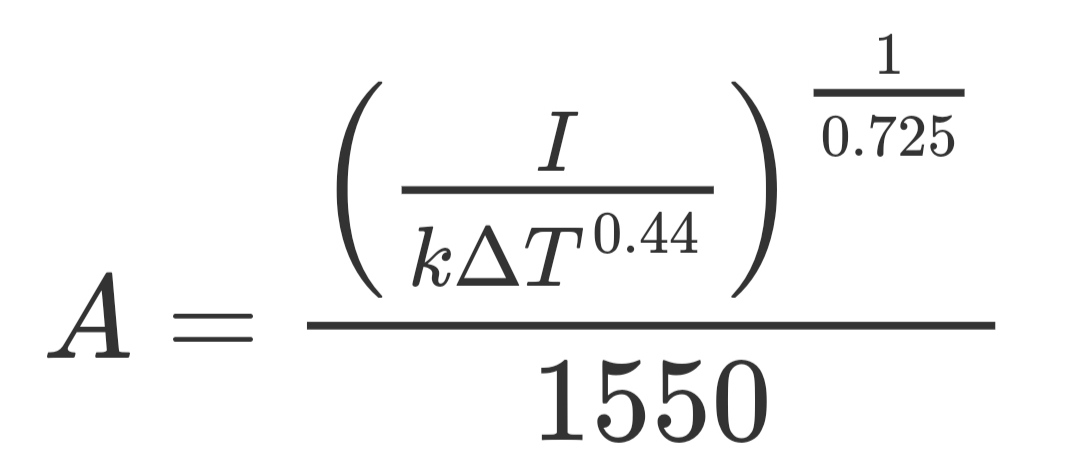
Based on the formula in MIL-STD-275E,
this calculator determines the required pattern cross-sectional area and trace width for a given current.
A: Cross-sectional area [mm²]
k: Coefficient based on the layer (0.024 for inner layers, 0.048 for outer layers)
ΔT: Temperature rise [°C]
I: Current [A]
this calculator determines the required pattern cross-sectional area and trace width for a given current.
A: Cross-sectional area [mm²]
k: Coefficient based on the layer (0.024 for inner layers, 0.048 for outer layers)
ΔT: Temperature rise [°C]
I: Current [A]
| Inner-layer cross-sectional area | mm² |
| Outer-layer cross-sectional area | mm² |
| Inner-layer trace width | mm |
| Outer Layer Trace Width | mm |
No customer feedback for this calculation yet.